

To-sun Technology · News Trends
Invite you to witness every step of development and growth
Technical Solution for the Construction of a Micro-Nano Processing Platform Laboratory - Nanjing Expansion Technology
Release time:
2025-07-17 11:05
I. Introduction
In today's rapidly developing technology, micro-nano processing technology, as the core support of many cutting-edge fields, is becoming increasingly important. From semiconductor chip manufacturing to the preparation of microscopic devices in biomedicine, from microelectromechanical systems (MEMS) to nano-material applications, micro-nano processing technology injects continuous impetus into technological innovation. To assist research institutions, universities, and enterprises in their in-depth exploration and innovation in the micro-nano field, Nanjing Expansion Technology Co., Ltd. With its rich experience and professional technical team, has participated in the construction of numerous micro-nano processing platforms, creating an ultra-high-precision experimental environment. Below is an introduction to the technical solutions for the construction of micro-nano processing platform laboratories.
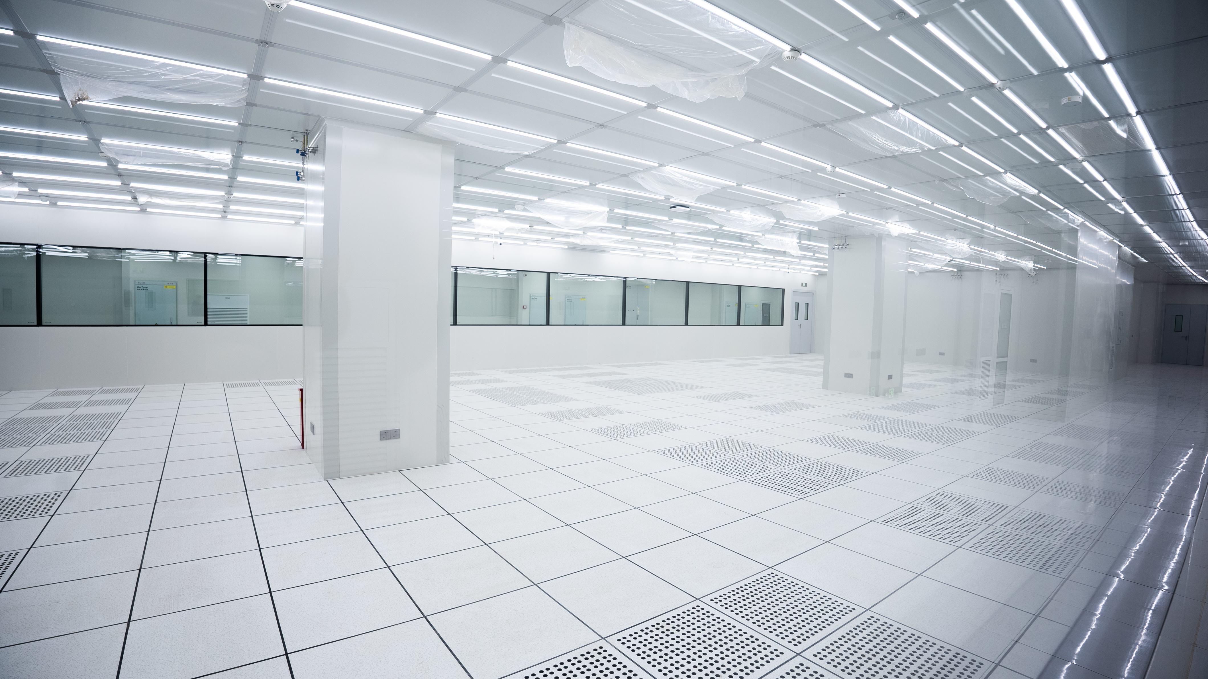
- Nanjing University (Suzhou) Micro-Nano Processing Platform, co-constructed by Nanjing Expansion Technology -
II. Core Positioning and Characteristics of the Micro-Nano Processing Platform Laboratory
The micro-nano processing platform laboratory is a comprehensive research and production hub integrating high-precision processing, advanced material preparation, and performance testing and analysis. It is a key carrier for promoting the transition of micro-nano technology from theoretical research to practical application. Its core positioning is to provide users with a full-process solution from micro-nano structure design and preparation to device integration and performance characterization, meeting the diverse needs of different fields for micro-nano scale materials and devices.
This platform laboratory has significant technical characteristics: First, cross-scale processing capabilities, which can achieve continuous scale processing from the micrometer to the nanometer level, covering the preparation needs from traditional MEMS devices to new nano-structures such as quantum dots and nanowires; second, multi-material compatibility, which can process and integrate a variety of materials such as semiconductors, metals, ceramics, and polymers, providing strong support for the research and development of heterogeneous material devices; third, modular design of processes, each processing and testing module is independent and can be flexibly combined, allowing for quick adjustment of the process route according to specific research projects or production tasks, greatly improving experimental efficiency; fourth, intelligent integration level, by introducing Internet of Things technology and automated control systems, real-time monitoring of equipment operation status, intelligent optimization of process parameters, and automatic acquisition and analysis of experimental data are achieved, providing a guarantee for high-precision and high-repeatability processing.
In terms of systematic advantages, the platform laboratory has established a complete quality control system, ensuring the reliability of processing precision and experimental results through strict standardized process management and regular equipment calibration; at the same time, relying on a professional technical service team, it can provide users with full-cycle technical support from process development and equipment operation to problem diagnosis, reducing the user's threshold. In addition, the platform emphasizes openness and sharing, and can achieve efficient utilization of equipment and technical resources through a reasonable resource scheduling mechanism, providing a high-quality platform for multidisciplinary cross-research and industrial collaborative innovation. The construction of the micro-nano processing platform laboratory will effectively solve the problems of equipment dispersion, process incompatibility, and high technical thresholds in the micro-nano processing field, providing strong technical support for basic research and industrial upgrading in fields such as microelectronics, optoelectronics, biomedicine, and new energy, and accelerating the transformation of scientific research achievements into actual productivity.
III. Laboratory Planning
3.1 Functional Zoning Design
- Lithography Area: As a key link in micro-nano processing, the lithography area is equipped with high-precision lithography equipment, including ultraviolet lithography systems and advanced electron beam lithography equipment. The former is suitable for mass production of larger micro-nano structures, with the advantages of easy operation and high efficiency; the latter can achieve ultra-high-resolution pattern transfer at the nanometer level, meeting the needs of research projects and high-end manufacturing that have strict requirements for small-size structures. At the same time, auxiliary equipment such as spin coaters and baking machines are equipped to ensure that the photoresist is evenly coated and solidified on the substrate, laying the foundation for high-quality lithography.
- Thin Film Deposition Area: This area has a variety of thin film deposition equipment, such as physical vapor deposition (PVD) systems, which can deposit metal, alloy, and compound thin films on the substrate surface through evaporation and sputtering, used to make electrodes, barrier layers, and other structures; chemical vapor deposition (CVD) equipment can grow high-quality semiconductor and insulating material thin films at lower temperatures, meeting the needs of different material systems and process conditions. In addition, molecular beam epitaxy (MBE) equipment can precisely control the atomic-level growth of thin films, preparing epitaxial layers with atomic-level flatness and precise composition control, suitable for the research and development of semiconductor quantum structures and new materials.
- Etching Area: Etching is an important means of removing unwanted materials to achieve precise shaping of micro-nano structures. The etching area is equipped with dry etching equipment, such as reactive ion etching (RIE), inductively coupled plasma etching (ICP), etc., which can achieve anisotropic etching of various materials, obtaining high aspect ratio fine structures; wet etching equipment is used for some etching processes with high selectivity requirements and large-area patterns. At the same time, corresponding etching endpoint detection systems are equipped to ensure precise control of the etching process and process repeatability.
- Cleaning and Pre-treatment Area: Before micro-nano processing, cleaning and pre-treatment of the substrate is crucial. This area is equipped with ultrasonic cleaners, megasonic cleaning equipment, and chemical cleaning tanks, which can effectively remove oil stains, particulate contaminants, and other impurities from the substrate surface, ensuring that the substrate surface reaches extremely high cleanliness. At the same time, surface pre-treatment equipment, such as plasma cleaners, is available to activate the substrate surface, enhancing the effect of subsequent thin film deposition, photoresist adhesion, and other processes.
- Testing and Characterization Area: To accurately evaluate the performance of micro-nano processed structures and devices, the testing and characterization area is equipped with a series of advanced analytical instruments. Scanning electron microscopy (SEM) is used to observe the surface morphology of micro-nano structures, with a resolution up to the nanometer level; atomic force microscopy (AFM) can accurately measure the microscopic morphology and mechanical properties of the sample surface; energy dispersive spectroscopy (EDS), X-ray photoelectron spectroscopy (XPS), etc., are used to analyze the composition and chemical state of materials. In addition, electrical testing systems and optical testing equipment are also available to meet the comprehensive testing needs of the electrical and optical properties of micro-nano devices.
- Auxiliary Functional Area: The auxiliary functional area includes material storage rooms, gas cylinder rooms, pure water preparation rooms, chemical storage rooms, etc. The material storage room is used to store various substrates, photoresists, masks, and other processing materials, classified and stored according to the properties and storage requirements of different materials to ensure the quality and safety of the materials. The gas cylinder room centrally stores special gases used in etching, deposition, and other processes, equipped with a complete gas leak detection and ventilation system to ensure the safe use of gases. The pure water preparation room prepares ultrapure water that meets the needs of micro-nano processing through multi-stage filtration, reverse osmosis, and other processes, used in cleaning, wet etching, and other process steps. The chemical storage room is used to store various chemical reagents, classified and stored according to the hazardousness of the reagents, and equipped with corresponding protection and emergency handling facilities.
3.2 Space Layout Planning
- Overall Layout Principles: Guided by the process flow, following the order of cleaning pretreatment, lithography, thin film deposition, etching, and testing and characterization, the positions of various functional areas are reasonably arranged to minimize and optimize the flow of materials and personnel, reducing cross-contamination and process interference. Meanwhile, sufficient consideration is given to the size, weight, installation, and maintenance requirements of the equipment, reserving adequate operating space and equipment transport channels.
- Cleanroom and Non-Cleanroom Division: Areas with high environmental cleanliness requirements, such as lithography, thin film deposition, and etching, are designated as cleanrooms, using a positive pressure air supply system to ensure that the air cleanliness in the cleanroom reaches a thousandth-grade or even a hundredth-grade standard. A buffer zone is set up between the cleanroom and the non-cleanroom. Personnel and materials entering and exiting the cleanroom must pass through the buffer zone for purification to prevent contaminants from the non-cleanroom from entering the cleanroom.
- Personnel and Material Flow Channel Design: Separate personnel and material flow channels are set up to avoid mutual interference between personnel and materials during movement. The personnel passage is equipped with an access control system to manage the access permissions of personnel entering the laboratory, ensuring the safety and order of the laboratory. The material passage is equipped with transfer windows, automated material handling systems, and other equipment to achieve efficient and clean transfer of materials between different functional areas.
- Equipment Layout Optimization: Based on the frequency of use and relevance of the equipment, the equipment is reasonably arranged. Frequently used equipment is placed in locations convenient for operation and maintenance, reducing the walking distance for operators. For equipment that generates vibration, noise, or waste gas, corresponding vibration isolation, sound insulation, and waste gas treatment measures are taken, and it is placed away from equipment sensitive to vibration and noise to avoid affecting other equipment and experimental processes.
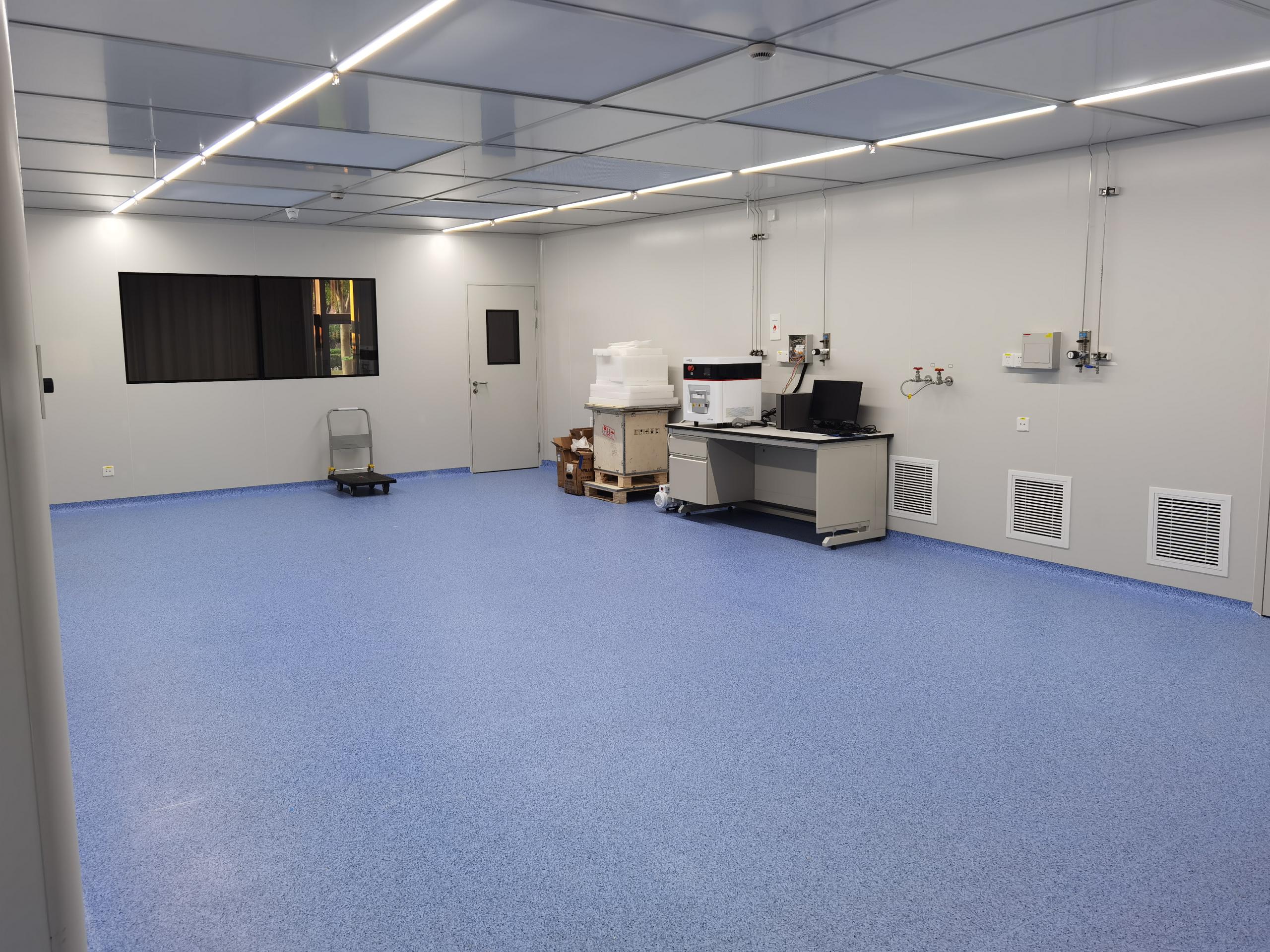
- Nanjing Expansion Technology participated in the construction of Zhejiang University (Haining) Micro-Nano Processing Platform -
IV. Equipment Selection and Configuration
4.1 Lithography Equipment
- Ultraviolet Lithography System: Select a UV lithography equipment with high resolution, large field of view, and high-precision alignment functions. For example, a certain brand's UV lithography system uses advanced optical exposure technology, with a resolution of up to 2μm, which can meet the lithography needs of most micrometer-level micro-nano structures. The equipment is equipped with an automatic alignment system, with an alignment accuracy of ±0.5μm, enabling multi-batch, high-precision lithography processing. It also has multiple exposure modes, such as contact exposure, proximity exposure, and projection exposure, allowing flexible selection according to different lithography process requirements.
- Electron Beam Lithography Equipment: To meet the needs of nanometer-level lithography, high-performance electron beam lithography equipment is selected. This equipment uses an electron beam to expose the photoresist, with a resolution of up to 10nm or less, capable of producing extremely fine nanostructures. Equipped with an advanced pattern generator and electron beam control system, it can achieve fast and accurate writing of complex patterns. It also features a high-vacuum environment and low-noise design to ensure the stability of the electron beam and lithography quality.
4.2 Thin Film Deposition Equipment
- Physical Vapor Deposition (PVD) System: A magnetron sputtering PVD device is configured, which can achieve sputtering deposition of various metals, alloys, and compound materials. The equipment is equipped with multiple sputtering targets, and the thickness and composition of the thin film can be precisely controlled by controlling parameters such as sputtering power and time. For example, a certain brand's magnetron sputtering PVD system can deposit metal thin films with uniformity better than ±2% on the substrate, and it has a quick target change function to improve production efficiency. In addition, an evaporation source can also be equipped to achieve evaporation coating processes, meeting the needs of different thin film preparation.
- Chemical Vapor Deposition (CVD) Equipment: A configuration scheme combining atmospheric pressure CVD (APCVD) and low-pressure CVD (LPCVD) equipment is selected. APCVD equipment is suitable for large-area, rapid thin film growth, and can deposit high-quality insulating material thin films such as silicon dioxide and silicon nitride in a short time. LPCVD equipment performs thin film growth at lower pressure, which can effectively improve the quality and uniformity of the thin film and is suitable for the growth of semiconductor material thin films. For example, a certain brand's LPCVD equipment can grow silicon epitaxial layers with thickness uniformity better than ±1%, meeting the needs of high-end applications such as integrated circuit manufacturing.
- Molecular Beam Epitaxy (MBE) Equipment: An ultra-high vacuum MBE system is used, equipped with multiple elemental sources and a precise beam current control system, which can achieve atomic-level precise epitaxial growth of III-V, II-VI, and other compound semiconductor materials. The equipment has real-time monitoring and feedback control functions, and can adjust the growth parameters according to the real-time monitoring data during the growth process to ensure the quality and performance of the epitaxial layer. For example, a certain brand's MBE equipment can grow quantum well structures with atomic-level flatness, used for the preparation of high-performance optoelectronic devices.
4.3 Etching Equipment
- Dry Etching Equipment: Reactive ion etching (RIE) and inductively coupled plasma etching (ICP) equipment are provided. RIE equipment is suitable for processes with high etching precision requirements and anisotropic etching, and can achieve fine etching of materials such as silicon, silicon dioxide, and silicon nitride. ICP equipment has higher plasma density and etching rate and is suitable for etching high aspect ratio structures, such as the manufacturing of MEMS devices. For example, a certain brand's ICP etching equipment can achieve a silicon etching aspect ratio of more than 10:1, and the etching uniformity is good.
- Wet Etching Equipment: Wet etching equipment with high automation and good etching selectivity is selected. The equipment is equipped with a precise temperature control system and chemical reagent delivery system, which can precisely control the etching temperature, reagent concentration, and etching time according to different etching process requirements. For example, when etching silicon materials, a certain brand's wet etching equipment has a silicon dioxide etching selectivity of more than 100:1, effectively protecting areas that do not need to be etched.
4.4 Testing and Characterization Equipment
- Scanning Electron Microscope (SEM): A high-resolution, large depth-of-field SEM device is selected, which can clearly observe the surface morphology of micro-nano structures. The equipment is equipped with a field emission electron gun, with a resolution of less than 1nm, which can be used to observe fine structures at the nanometer level. It also has multiple signal detectors, such as secondary electron detectors and backscattered electron detectors, which can provide rich material information.
- Atomic Force Microscope (AFM): An AFM device with high resolution and multiple imaging modes is selected. The equipment can measure the microscopic morphology of the sample surface with atomic-level resolution, and can also perform force spectrum analysis, surface electrical property measurement, etc. For example, a certain brand's AFM equipment has a resolution of 0.1nm in tapping mode, which can be used to study the surface structure and properties of nanomaterials.
- Energy Dispersive Spectroscopy (EDS) and X-ray Photoelectron Spectroscopy (XPS): EDS is used to analyze the elemental composition of materials, and it is characterized by its speed and accuracy. XPS can perform in-depth analysis of the chemical states on the material surface, determining the chemical bonding state and content of elements. For example, a certain brand of EDS equipment can complete qualitative and quantitative analysis of samples within minutes, and the energy resolution of XPS equipment can reach 0.1 eV, enabling precise analysis of the chemical structure of the material surface.
- Electrical Testing System: Equipped with high-precision semiconductor parameter analyzers, probe stations, and other equipment, it can perform comprehensive testing of the electrical performance of micro-nano devices, such as current-voltage characteristics and capacitance-voltage characteristics. For example, a certain brand of semiconductor parameter analyzer can provide high-precision voltage and current sources, with measurement accuracy reaching the picoampere and microvolt levels, meeting the testing needs of tiny current and voltage signals.
- Optical Testing Equipment: Using spectral analyzers, optical power meters, microscopes, and other optical testing equipment, the optical performance of micro-nano optoelectronic devices can be tested, such as spectral response and optical power transmission. For example, a certain brand of spectral analyzer covers the ultraviolet-visible-near-infrared band, with a wavelength resolution of 0.1 nm, and can be used to analyze the spectral characteristics of optoelectronic devices.
V. Environmental Control System
5.1 Cleanroom Design
- Cleanliness Level: According to the requirements of micro-nano processing technology, the cleanliness level of key areas such as lithography, thin film deposition, and etching is set to Class 100, while the cleanliness level of testing and characterization areas and auxiliary functional areas is set to Class 1000. A vertical unidirectional flow or horizontal unidirectional flow airflow organization form is adopted to ensure uniform airflow in the cleanroom, effectively removing dust particles and other pollutants.
- Air Filtration System: The cleanroom air supply system uses three-stage filtration. The primary filter removes large dust particles, the medium filter further removes smaller particulate pollutants, and the high-efficiency particulate air (HEPA) filter achieves a filtration efficiency of over 99.97% for particles larger than 0.3 μm, ensuring that the air entering the cleanroom meets extremely high cleanliness standards. At the same time, the filters are regularly inspected and replaced to ensure filtration effectiveness.
- Positive Pressure Control: The cleanroom maintains positive pressure, and the pressure difference with adjacent areas is controlled between 5-10 Pa to prevent external pollutants from entering the cleanroom through doors, windows, and gaps. By installing pressure difference sensors and automatic regulating valves, the positive pressure value of the cleanroom is monitored and controlled in real-time, ensuring the stability of positive pressure control.
5.2 Temperature and Humidity Control
- Temperature Control: Micro-nano processing technology is very sensitive to temperature changes, so the laboratory is equipped with a high-precision temperature control system. Using a constant temperature and humidity air conditioning unit, through cooling, heating, humidification, and dehumidification functions, the laboratory temperature is controlled within the range of 22 ± 1 ℃, and the temperature fluctuation is controlled within ± 0.5 ℃/h. For equipment with extremely high temperature requirements, such as lithography and electron beam exposure, independent high-precision temperature control units are set to ensure the temperature stability of the equipment's working environment.
- Humidity Control: Humidity also has an important impact on the adhesion of photoresist and the growth quality of thin films. The laboratory's humidity control system controls the relative humidity within the range of 40%-60%, and the humidity fluctuation is controlled within ±5%. By installing humidity sensors and humidity regulating equipment, the laboratory humidity is monitored and adjusted in real-time to ensure the smooth progress of micro-nano processing technology.
5.3 Vibration and Noise Control
- Vibration Control: To reduce the impact of external vibrations on micro-nano processing equipment, the laboratory adopts various vibration isolation measures. The building is designed with foundation vibration isolation, and vibration isolation pads and spring isolators are used to isolate the building from ground vibrations. For equipment sensitive to vibration, such as lithography and electron microscopes, independent vibration isolation platforms are set up, using air spring isolation and rubber isolation technologies to control equipment vibration to an extremely low level. For example, for electron beam exposure equipment, the vibration is controlled below the VC-F class standard to ensure normal operation and high-precision processing.
- Noise Control: By selecting low-noise equipment, performing sound insulation treatment on equipment, and setting up sound insulation walls, the laboratory noise is controlled below 65dB (A). For equipment that generates relatively large noise, such as vacuum pumps and fans, sound insulation hoods and silencers are used to reduce noise interference to experimental personnel and the experimental process.
5.4 Waste Gas and Wastewater Treatment
- Waste Gas Treatment: The waste gas generated by the laboratory mainly includes acidic waste gas, alkaline waste gas, and organic waste gas. Corresponding waste gas treatment equipment is used for different types of waste gas. Acidic waste gas is neutralized by an alkaline solution spray tower, alkaline waste gas is neutralized by an acid solution spray tower, and organic waste gas is treated by activated carbon adsorption and catalytic combustion. Ensure that waste gas emissions meet national environmental protection standards and reduce environmental pollution.
- Wastewater Treatment: The wastewater from the laboratory mainly includes acidic wastewater, alkaline wastewater, and heavy metal-containing wastewater. The wastewater treatment system uses neutralization, sedimentation, filtration, and ion exchange processes to treat different types of wastewater. The treated wastewater is discharged after meeting the discharge standards. For recyclable wastewater, reverse osmosis and other technologies are used for recycling, achieving the recycling of water resources.
VI. Laboratory Management System
6.1 Equipment Management
- Establishment of Equipment Inventory: A detailed inventory is established for all equipment in the laboratory, recording information such as equipment name, model, manufacturer, purchase time, equipment number, technical parameters, instruction manuals, and maintenance records, facilitating equipment management and maintenance.
- Development of Equipment Maintenance Plan: Based on equipment usage and manufacturer recommendations, a reasonable equipment maintenance plan is developed. Regular maintenance, calibration, and repair work are performed on the equipment to ensure normal operation and stable performance. At the same time, equipment maintenance records are established to record the time, content, and maintenance personnel of each maintenance, facilitating tracking of equipment maintenance history.
- Equipment Failure Reporting and Handling: An equipment failure reporting mechanism is established. When equipment malfunctions, operators can report the failure through the online reporting system or telephone. After receiving the repair information, maintenance personnel should respond within the specified time and quickly diagnose and repair the equipment. For major equipment failures, experts should be organized for consultation to develop solutions and ensure that the equipment is restored to normal operation as soon as possible.
6.2 Personnel Management
- Personnel Training and Qualification Certification: Comprehensive training will be provided to all personnel entering the laboratory, including safety operating procedures, equipment operation skills, and experimental processes. Upon successful completion of the training, corresponding qualification certificates will be issued. Only qualified personnel are permitted to operate the relevant equipment and conduct experiments. Regular retraining will also be conducted to ensure that personnel's operational skills and safety awareness remain at a high level.
- Personnel Access Management: Different personnel access levels will be set based on personnel's job positions and responsibilities. For example, laboratory managers will have the highest level of access to equipment management, personnel management, and experimental data management; equipment operators will have access to equipment operation and daily maintenance; and experimental personnel will have access to conduct experiments on designated equipment. Personnel access management ensures the safety and order of the laboratory.
- Personnel Assessment and Incentive Mechanism: A personnel assessment mechanism will be established to regularly assess personnel's work performance, experimental results, and safe operation. Outstanding personnel will receive corresponding rewards, such as bonuses and certificates of merit; underperforming personnel will receive criticism, education, and training to encourage improvement. The assessment and incentive mechanism will enhance personnel's work enthusiasm and sense of responsibility.
6.3 Experiment Process Management
- Experiment Reservation and Scheduling: Experimental personnel will reserve experiments through the laboratory management system, filling in information such as the experimental project, required equipment, and experimental time. The laboratory manager will schedule experiments based on equipment usage and personnel reservation information, reasonably arranging equipment and experimental time to improve laboratory efficiency.
- Experiment Process Monitoring: During the experiment, real-time monitoring of the experimental process will be conducted through the installation of monitoring cameras and equipment operation status monitoring systems. This ensures that experimental personnel conduct experiments according to operating procedures, preventing equipment damage or experimental accidents caused by improper operation. Real-time data acquisition and recording can also be performed for subsequent data analysis and processing.
- Experimental Data Management: An experimental data management system will be established to centrally store, manage, and analyze data generated during experiments. Experimental personnel can upload experimental data through the system and set data access permissions to ensure data security and confidentiality. The system has data query, statistical analysis, and report generation functions, providing strong support for the evaluation of experimental results and the summarization of scientific research achievements.
For more information on the construction of micro-nano processing platform laboratories, please contact Nanjing Expansion Technology Co., Ltd.
Related News

Committed to becoming a leader in the field of laboratory construction in China

WeChat Public Number
Nanjing To-Sun Technology Co.,Ltd
sale@to-sun.com
Address: 6th Floor, Anke Building, 31 Guangju Road, jianye district, Nanjing